EddyCus® TF Series (Thin-Film) comprises a set of devices for real-time testing of the sheet resistance of thin films utilizing contact free eddy current testing technology. The systems can also be used for characterization of sensitive films and hidden or encapsulated layers on glass, wafers, or foils. Applications include:
- Sheet resistance testing from 0.1 mOhm/sq to 3,000 Ohm/sq
- Layer thickness measurement of metal-films from 5 nm to 500 microns
- Conductivity mapping from 1% IACS (0.6 MS/m)
Non-contact Sheet Resistance Measurement Solutions
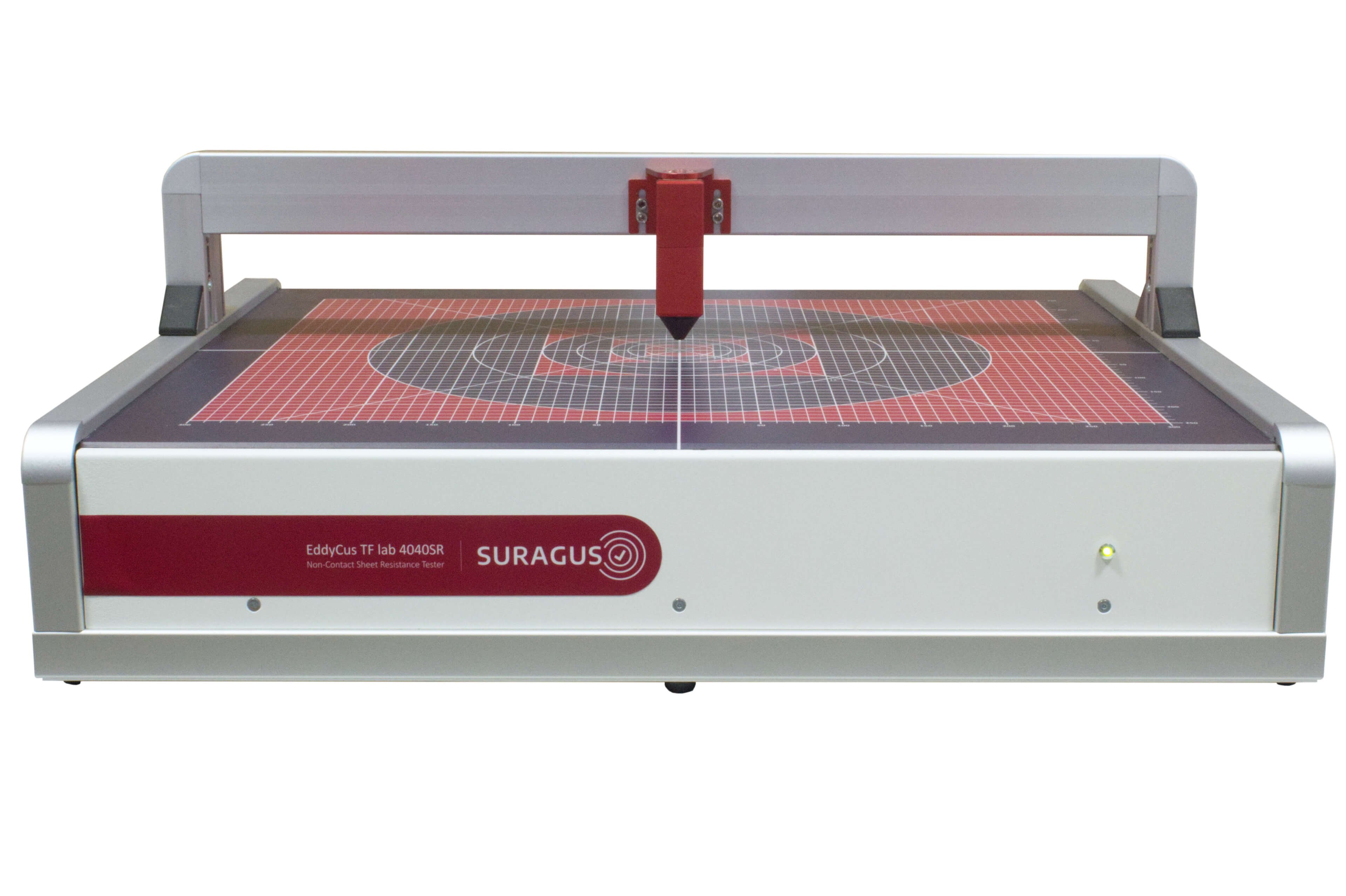
EddyCus® TF lab devices are sheet resistance and thickness measuring desktop systems designed for rapid non-contact thin film characterization in laboratories, R&D centers, and quality assurance departments in factories and fabs.
REQUEST QUOTE
Testing Applications
- Sheet resistance/resistivity testing for the assessment of deposition processes, annealing processes, doping processes, ablation processes, or oxidation processes (aging)
- Thickness testing of metal films
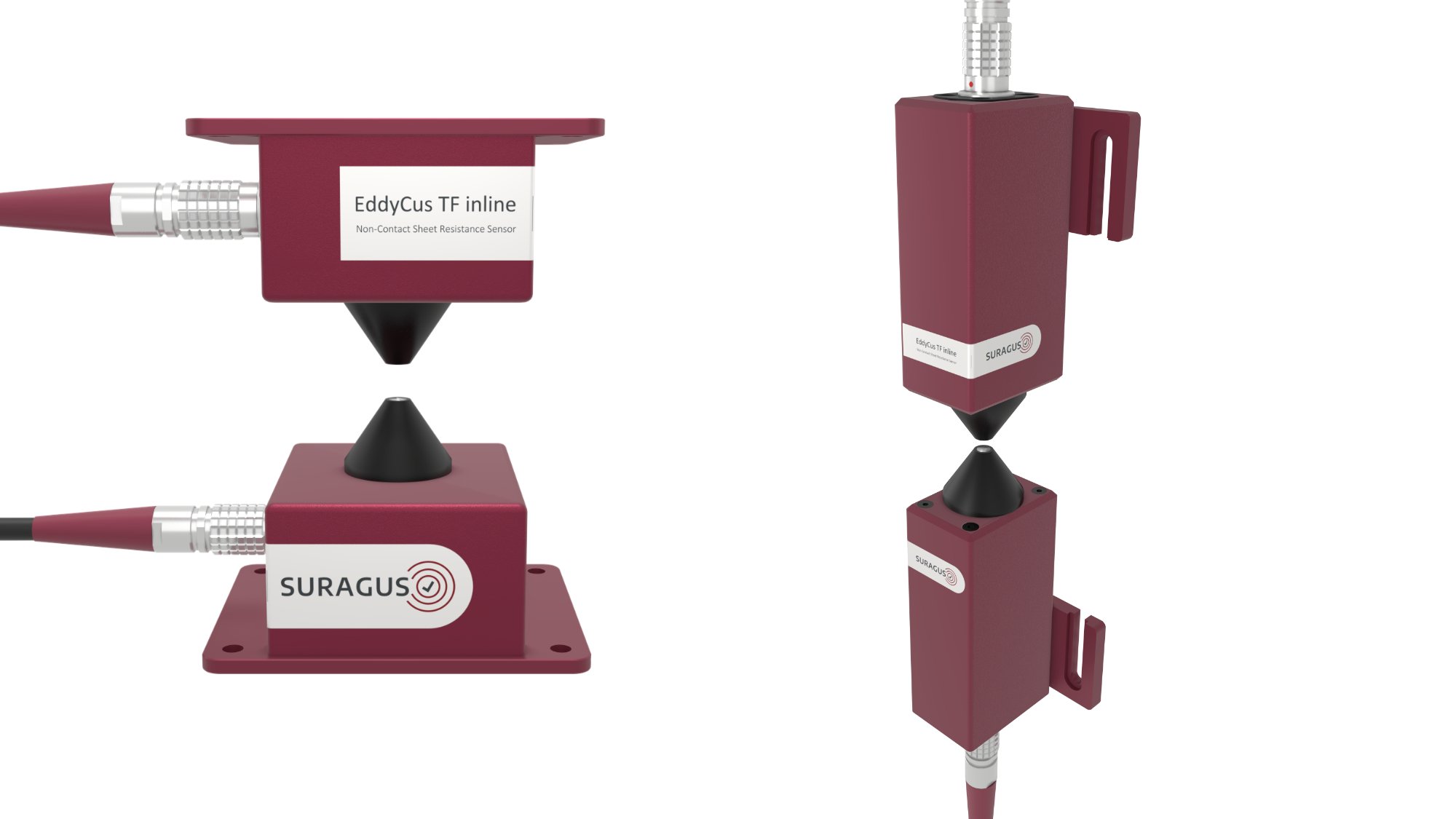
The EddyCus® TF inline series comprises integration kits for coating equipment enabling contactless inline sheet resistance monitoring and process controlling for deposition processes of conductive thin films.
REQUEST QUOTE
Testing Applications
- Inline sheet resistance measurement and optimization of target utilization
- Inline coating thickness measurement of metallic thin films
- Substrate thickness measurement
- Crack detection, wafer testing, and material sorting
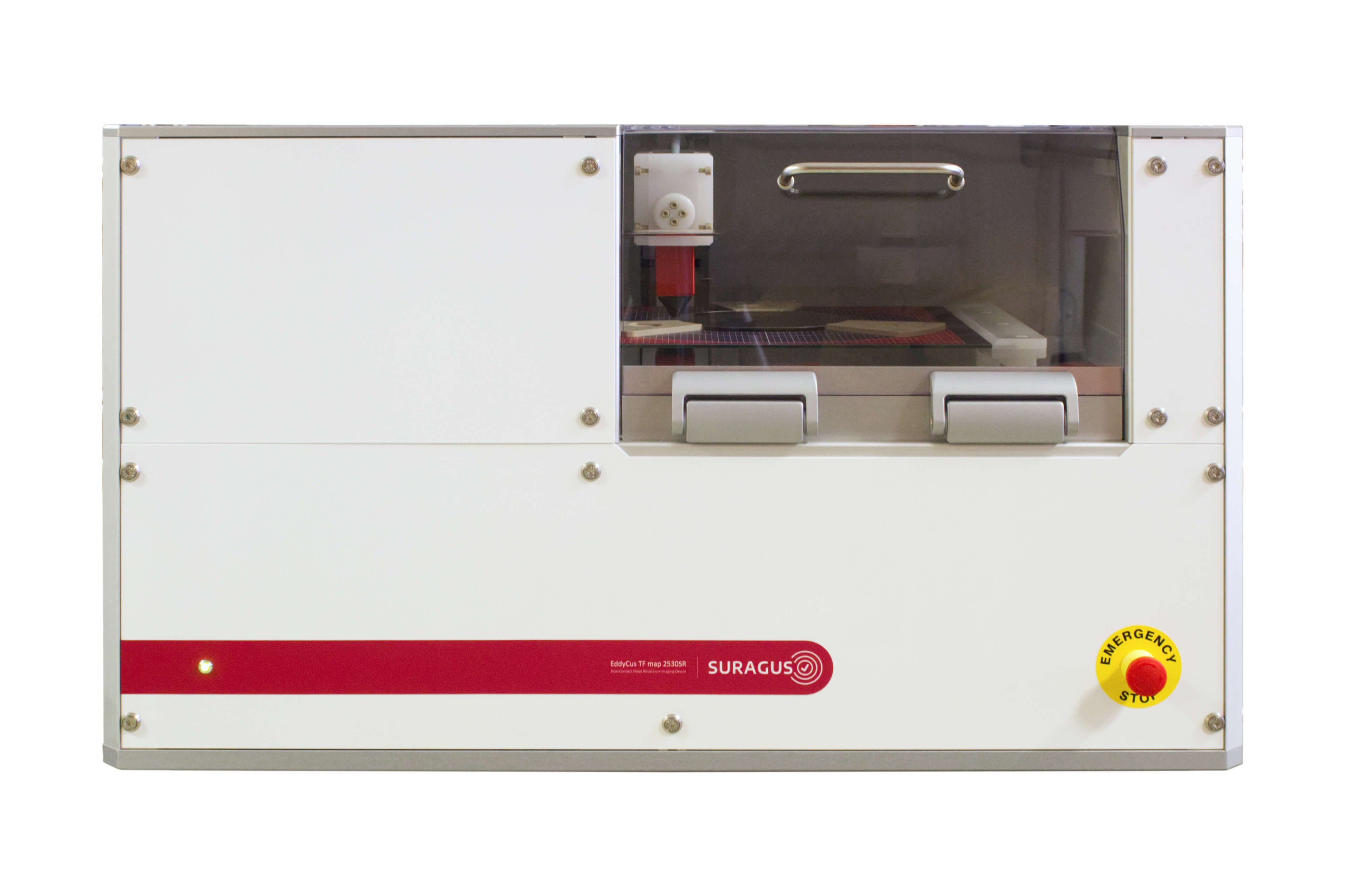
The EddyCus® TF map series is designed for rapid mapping of sheet resistance, assessment of layer homogeneity, and detection of local effects and defects. Systems are available as free standing test stands or desktop devices.
REQUEST QUOTE
Testing Applications
- Sheet resistance mapping of TCO/TCMs, metals, and wafers
- Layer thickness mapping of metallic thin films
- Homogeneity mapping and defect detection (e.g. impurities, cracks, deposition effects)
- Assessment of structured conductive thin films
- Crack detection, wafer testing and material sorting
Materials & Industries
Transparent Films
- TCO (ITO, FTO, AZO, ATO)
- CNT (carbon nanotubes)
- Metal nano-wires
- Graphene films
- Other
Metallic Films
- Copper
- Aluminium
- Molybdenum
- Zinc
- Silver
- Other
Fields of Application
- Architectural/float glass industry
- Packaging foils & materials
- PV/Solar & antistatic foils
- Touch screens & flat monitors
- LED/OLED & Smart-Glass applications
- Semiconductor industry
- De-icing & heating applications